Within WP1 of the EU funded project SiTaSol AIXTRON SE and AIXTRON Limited investigate and develop low cost III-V epitaxy processes and reactor concepts. In focus of research are investigations and developments on metal organic chemical vapor deposition (MOCVD) reactors to increase growth rate of Ga(In)As(P) and to improve production cost.
The main objectives of WP1 are:
- to validate scalable epitaxy processes for the III-V absorber layer deposition at very high growth rates, deposition efficiencies and group V utilization, compatible with the cost targets of current market.
- to investigate waste treatment and recycling methods for hydrogen and metals originating from the III-V growth which are compatible with the current cost targets for wafer.
- to validate scalable processing routes for III-V/Si tandem solar cells which are compatible with the performance and cost targets.
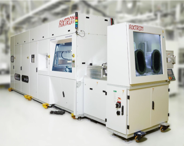
The Figure above shows picture with front right view of an AIXTRON MOCVD Equipment, which is the basic tool for the project investigations and developments.