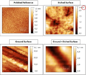
Process route A which is investigated within the SiTaSol-project follows the direct growth of the III-V absorber layers on low-cost silicon substrates. Avoiding the usual chemical-mechanical polishing steps allows a drastic cost reduction of the surface finishing process of the silicon cell. Different preparation routes containing specific grinding and/or etching steps have tested. The corresponding AFM images of the surfaces compared with a polished reference shows the figure below. Especially combinations of low-cost grinding plus etching appear promising for good epitaxial growth results.
Low Cost Si Substrate Preparation and GaAs Reuse - Update December, 2018
- Leif Jensen, TOPSIL Globalwafers A/S
- December, 2018