Objectives and Status
The front side electrodes of III-V solar cells comprise of metal grid lines on a patterned CAP. The task is to develop industrially scalable low cost processes for the front contact grid deposition suitable for tandem solar cells.
Task
Reducing the total series resistance of electrodes (contact resistance and bulk-resistance):
-
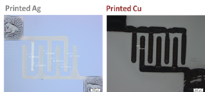
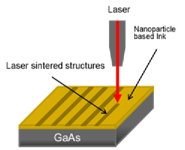
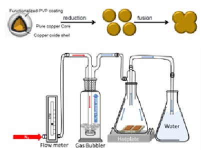
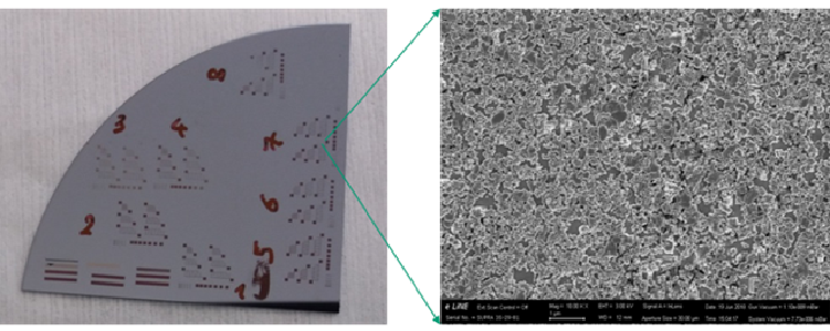
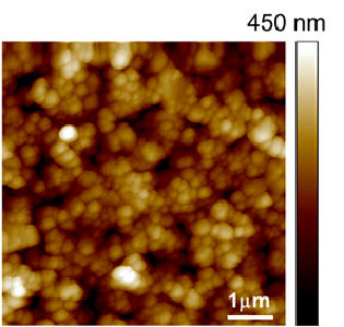
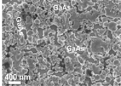
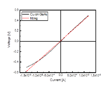
Metal inks were applied as contacts on the surface of GaAs by inkjet printing and spin coating.
-
Two sintering methods (laser and reducing atmosphere) for metal NP inks were developed. With respect to environmental impact; laser sintering is so far a more promising process.
-
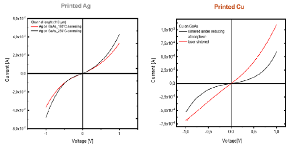
Ohmic contact behavior is observed in first results. Further activities to achieve an optimized contact resistance are ongoing.
Task
Development of bonding processes as an interconnection between top and bottom cells with high transparency and low contact resistance.
-
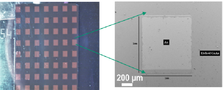
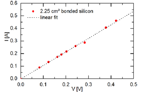
TCO thin films were spray-coated on highly doped Si and III-V epi layers and then annealed.
-
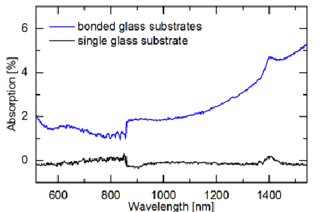
The quality of the applied TCO bonding films was investigated with electrical, mechanical (Maszara blade) and optical microscope characterization. Low resistance ohmic contact can be achieved for Si substrates. A high transmission is realized for the demanded wavelengths in general.
-
With respect to mechanical stability, a high bond strength is observed. Further investigations will focus on improving the contact resistance on III-V materials as well as on bond homogeneity.